BaseJump Socket 352
See this github link.
Below are:
- the definitions of the padring for the BaseJump 352-pin Open Source Socket (BaseJump Socket 352) interface.
- an open source substrate for a BGA substrate that adheres to BaseJump Socket 352
Back to main BaseJump page.
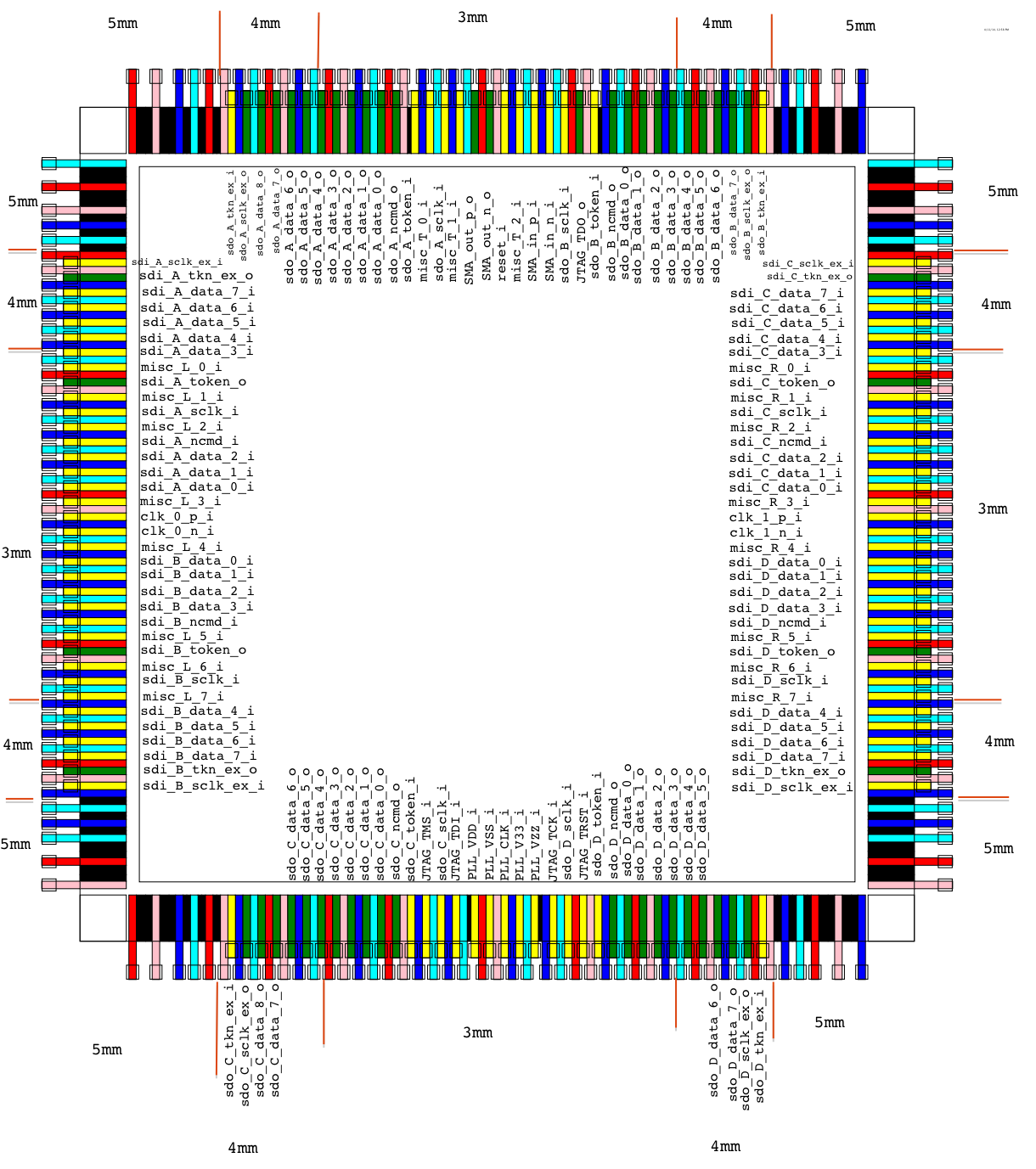
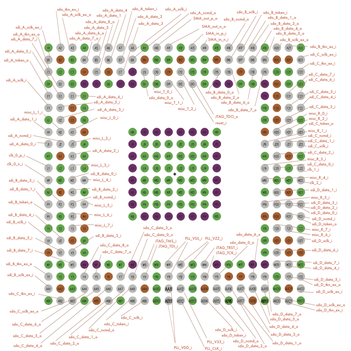
Padring
Often times VLSI chips
have a metal stack that is lower resistance in one direction than another. You should align the low resistance
direction so that it connects to the sides of the pad ring, as they have more connections to core Vdd/Vss.
We place outputs on the top/bottom of the padring, and allocate more I/O Vdd/Vss to these sides.
Separating inputs and outputs reduces noise on inputs.
The markers indicate which part of the pad out you would keep for each size of die (e.g. 3x3,4x4,5x5).
For smaller die, some bond wires will not be attached.
The ball out of the package is fixed and cannot be changed.
If you do repurpose the package and have not designed
a package before, we suggest you keep the BaseJump Socket Interface (pad ring arrangement) we have
on the diagram, and maintain the direction
and type of the pin (i.e. input, output, core Vdd, core Vss, I/O Vdd, I/O Vss), and also try to assign similar
purposes to each pin.
Your I/Os should have the same position relative to the middle of the side, but depending on die size, will be further or closer to the center of the die.
For historical use, or for package modeling:
These are the input specification we gave the substrate designer.
These are the output geometrical specs given back to us by the substrate designer.
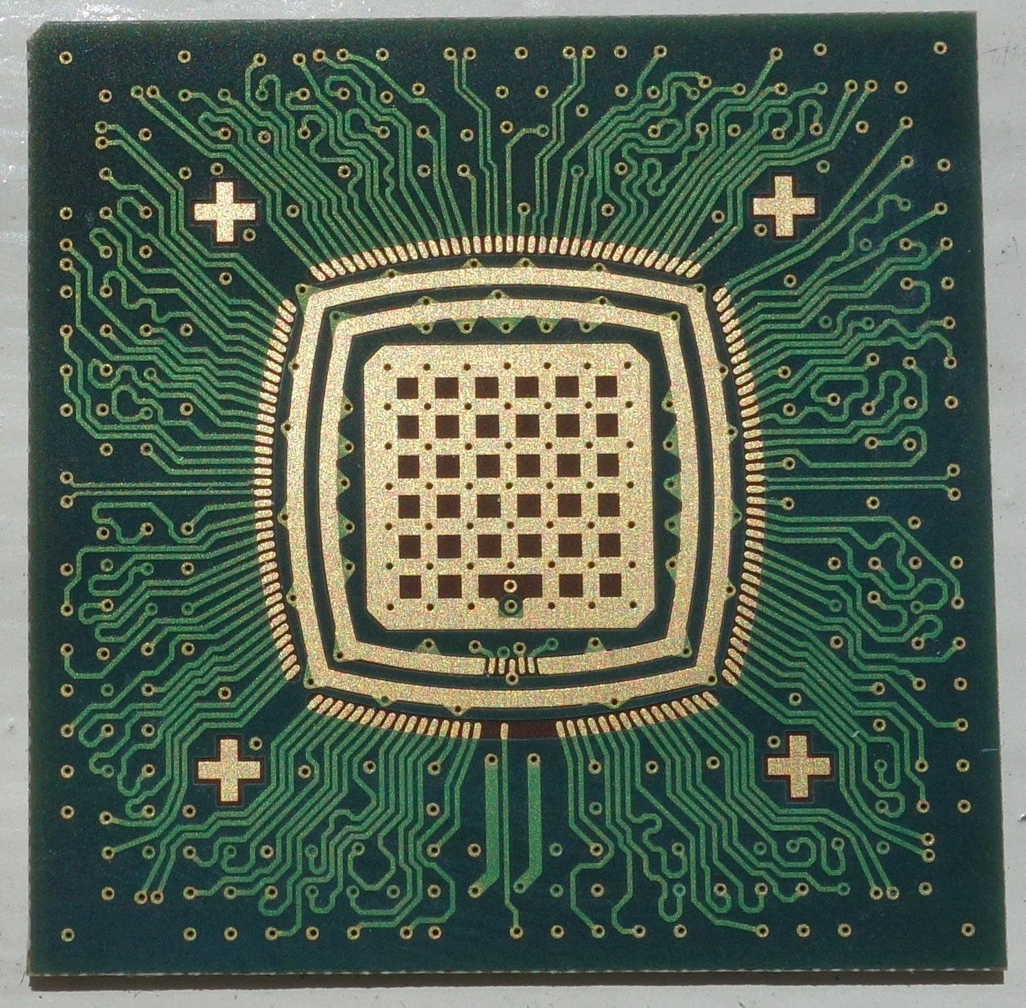
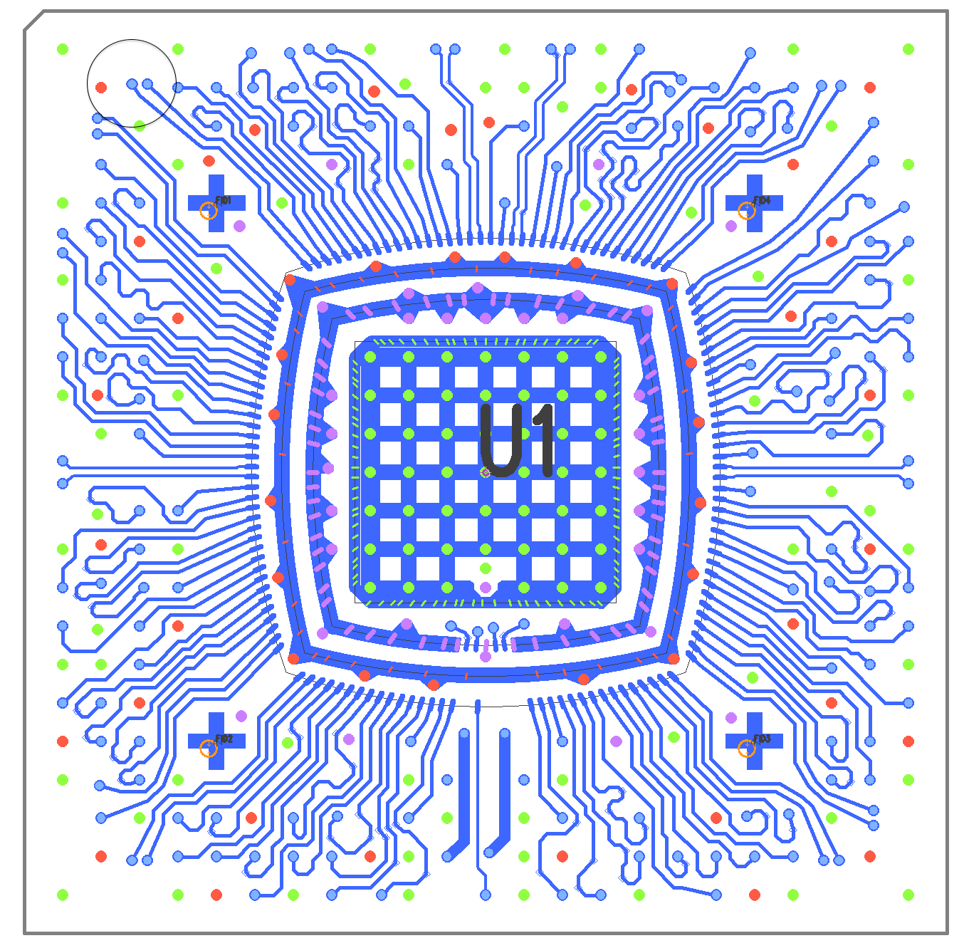
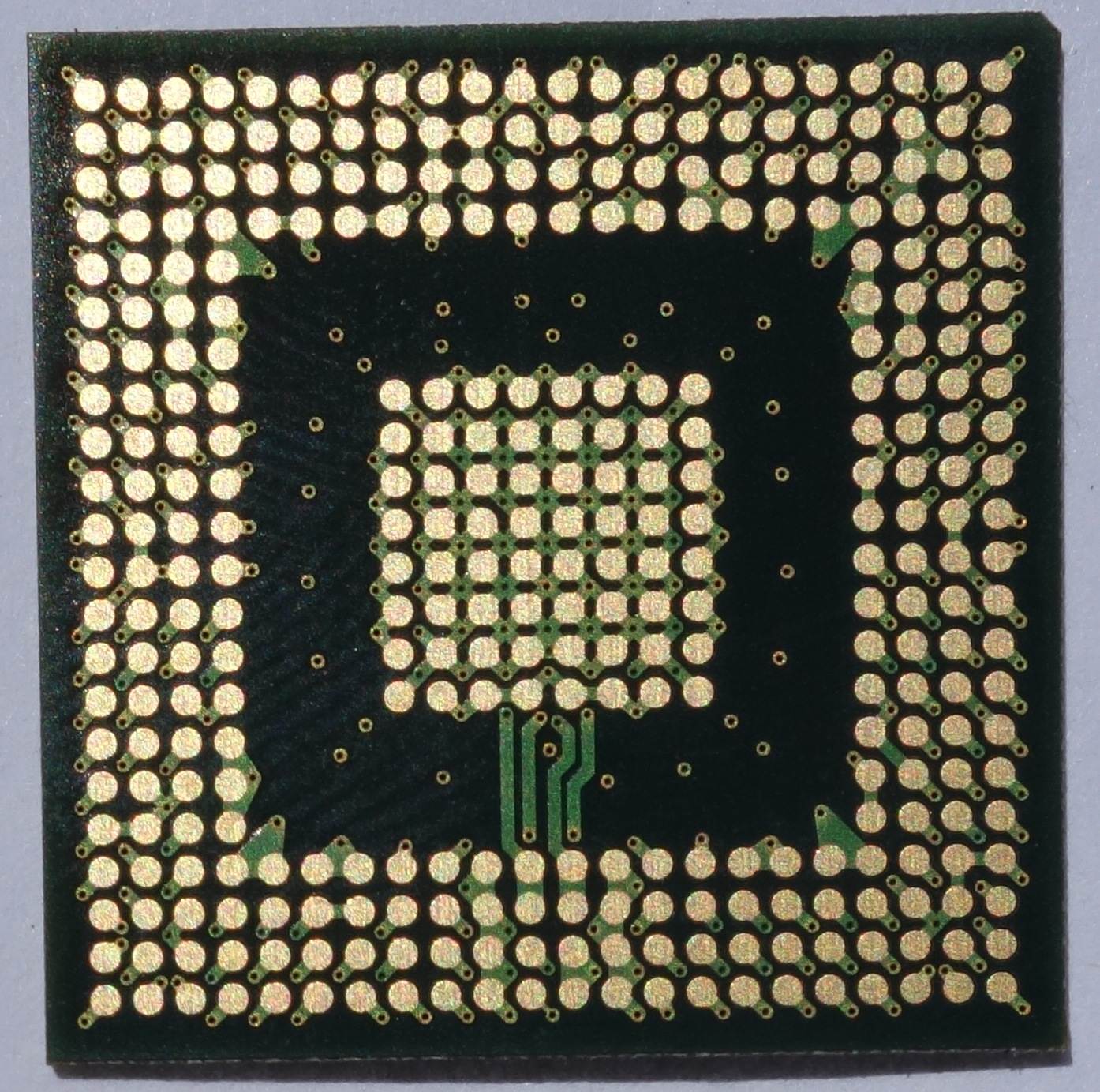
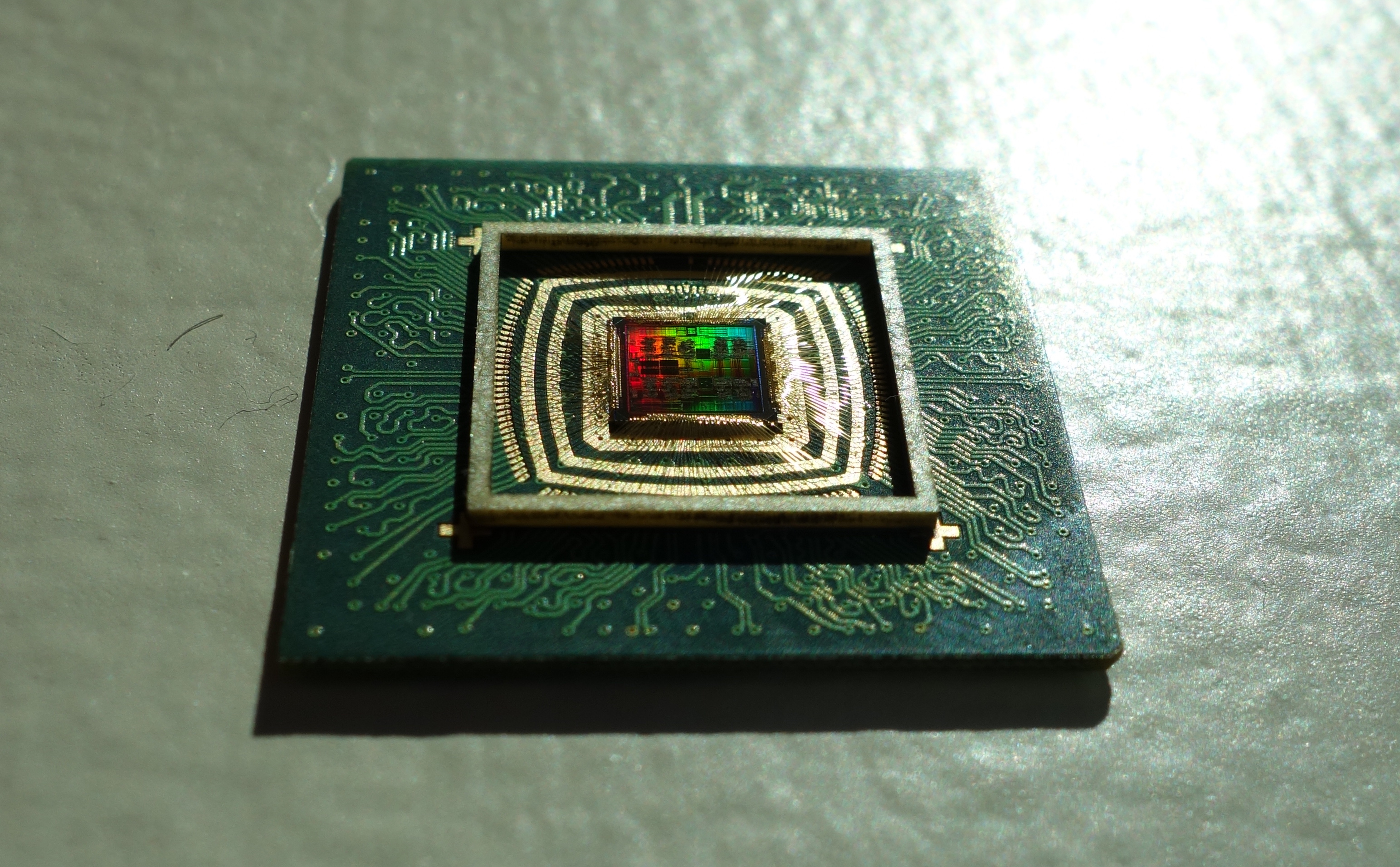
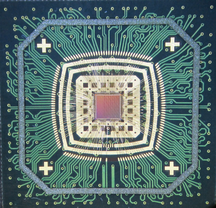
BaseJump Socket 352 Ball Grid Array (BGA) Package Substrate
To use your silicon, you need a package.
High-performance packages are in short supply in academia;
typically people ar
e relegated to using low-performance
PGA, QFP or QFN packages.
To support BaseJump Socket, we created a wirebond Ball Grid Array (BGA) package that can be broadly used.
It has special features that allow it to be adopted across
many different chip designs.
It is suitable for chips between 3x3 mm and 6x6 mm
but is most optimized for 4x4 mm and 5x5mm.
You can provide our package geometry file and your bondpad
coordinates to your wirebonding house, and they will tell you
if it is bondable.
Traces are length-matched and impedance controlled, there is a section for PLL,
and separate voltage rails for I/O and Core VDD. Although mostly re-purposable,
signal wires have special capabilities (e.g. clock, pll, jtag, flow control credits)
that you can take advantage of if you do assignment correctly.
High-speed 100-ohm differential pairs are provided for clocks or other purposes.
We can provide advice for you on how to assign your signals, just email.
| Bond Wires | Balls
|
| Connections to Substrate Bond Pads that go to individual balls | 144 | 144
|
| Connections to BGA internal VDD, I/O VDD, VSS and I/O VSS Planes/Rings | 188 | 39, 41, 40, 88
|
|
|
| Total | 332 | 352
|
NOTE: Image of bottom side on right is a "top-down" x-ray style view, and is reversed with regard to the actual photo on the left.
Example: BSG Ten, a 10-core manycore RISC-V chip in 180nm, 5x5mm
See this link" for more details.
Example: Outerspace, a sparse matrix multiply chip in 40nm, 3x3mm
Note that two I/Os on each corner are not used since it is a small die,
but not that many.