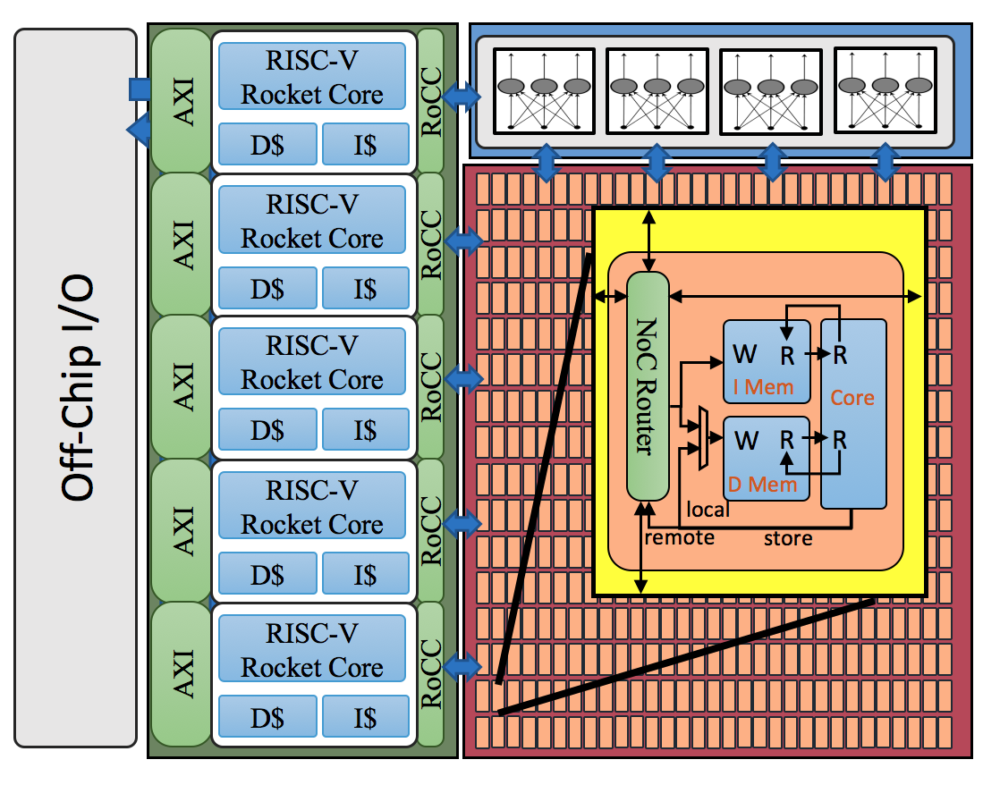
Welcome to BaseJump Manycore.

Brought to you by Taylor's Bespoke Silicon Group.

Code

See bsg_manycore GitHub git repo.

BaseJump Manycore makes use of BaseJump STL, and
BaseJump FPGA Bridge as well.

See our Quickstart guide for using Celerity, the open source 511-core chip. The Celerity tapeout was funded by the DARPA CRAFT program.

Since then, we have been a part of the DARPA SDH program and have been improving the architecture to make it more programmable using a CUDA-like language. The latest version is called HammerBlade Manycore. See bsg_manycore GitHub git repo for the latest code and documentation. A 14- nm prototype was taped out in August 2019. It is a ridiculously awesome chip.

Publications

See these publications for more details: Contact prof.taylor@gmail.com for more details.

We are looking for collaborators who are excited about developing programming methodologies for and using manycore chips.

e.g., Remote Store Programming, Streaming, CUDA, OpenCL, Halide, OpenSHMEM...


Email prof.taylor@gmail.com

496-core BaseJump Manycore (@ 1.4 GHz) in Celerity Chip (16nm TSMC FinFet technology)

BaseJump Manycore has been combined and used in the 511 RISC-V Core Open Source Celerity
chip which was taped out in TSMC 16nm FinFet technology in April 2017.

The pictures below are the chip layout, the architectural diagram, and the 16nm silicon:

.    


Click here for a super high-res layout of the chip.


Celerity couples the 1.4 GHz 496-core BaseJump Manycore array to 5 Rocket cores via independent RoCC links. It also has a neural network accelerator with multiple connections to the manycore. The manycore can do stores that traverse across the mesh and write directly into the neural network state. The daughterboard in the picture below is the Celerity system running. The Zedboard on the right provides DRAM and ethernet connectivity.


On the same chip, there is also a 10-core version of the manycore in a low-voltage domain, which was first prototyped below in Dec 2016:

10-core RISC-V BaseJump Manycore in "BSG Ten" ASIC (180 nm TSMC)

Taylor BSG teammembers (Scott Davidson, Chun Zhao, Shaolin Xie and Michael Taylor) have also taped out a 10-core manycore in TSMC 180 (commit_tag).

This chip multiplexes the the south side of the manycore directly to the off-chip I/O interface using the T block. An FPGA can be used to extend the manycore in the south direction, or alternatively you can couple the manycore to a processor inside an FPGA.

Connectivity looks like this:

                  
                Connectivity                    
Tile 0Tile 1
Tile 2Tile 3
Tile 4Tile 5
Tile 6Tile 7
Tile 8Tile 9
T
/\
A
/ / / | | \ \ \
I O I O I O I O
Key:

LabelBlock
0-9RISC-V Cores 0..9
I8-bit High-Speed Source Synchronous Input DDR channel
O8-bit High-Speed Source Synchronous Output DDR channel
CClock generator
AAssembler (combines 4 8-bit channels into wide 32-bit channel)
TTunnels two southern most network links as independent logical channels to off-chip FPGA
/Cross-chip channels


(Click on the pictures for larger view.)

Click here for zoomed-in photos of the chip.


Shmoo plot confirming operation at 280 MHz @ 1.8V and 370 MHz @ 2.4V


Our High-Speed Singled-Ended DDR I/O (using off-the-shelf 3.3V TTL) has been confirmed to work at ~390 MHz with 16mA outputs.


Back to BaseJump mainpage.