BaseJump Motherboards for BaseJump Socket 352
Click to go to main bjump.org website.
Git repo is here.
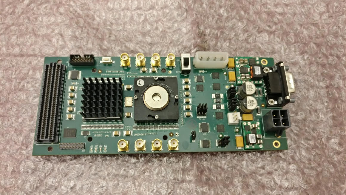
BSG RealTrouble
This is the first BaseJump Socket 352 compliant motherboard.
It contains Socket 352 ASIC as well as an Spartan-6 FPGA, called the Gateway FPGA.
It supports connection to Xilinx host boards via the high-speed FMC connector,
for use of off-chip DRAM, PCI-e, Ethernet, etc.
The Gateway FPGA has the code for controlling the on-board power supplies,
and for forwarding data between the full-duplex high-speed source-synchronous DDR
link (called BaseJump FPGA Bridge) to the Socket 352 ASIC and the LPC FMC connector (which goes to an ML-605 or similar Xilinx XUP host.)
It also provides resources for clock generation.
Spartan-6 was used to keep the cost low ($200 for the GW FPGA), and because it allows
a large voltage range (up to 3.3V) for I/O's, and because it allows tuning of both input
and output delays, allowing for high-speed I/O. Termination is external for debug probing
and to allow heat to dissipated outside of the chips, which are wirebond BGA and only have 3W budgets.
The board has (unless noted, these are connected to the GW FPGA):
- LPC FMC connector with ~16 differential pairs (plus clock) in each direction (~ 1 GHz)
- RS-232 port
- JTAG connector
- 8-pin header for communication in either direction to GW FPGA, or for jumpers
- 4 SMA pairs:
- two (one in, one out) are connected to the ASIC FPGA, and
- two (one in, one out) are connected to the GW FPGA.
The traces on these pairs are 100-ohm impedance and inputs are terminated with a 100-ohm resistor.
- various LEDs
- header for powering fan
- header for powering board externally
- programmable power supplies and power measurement for ASIC core and I/O voltage
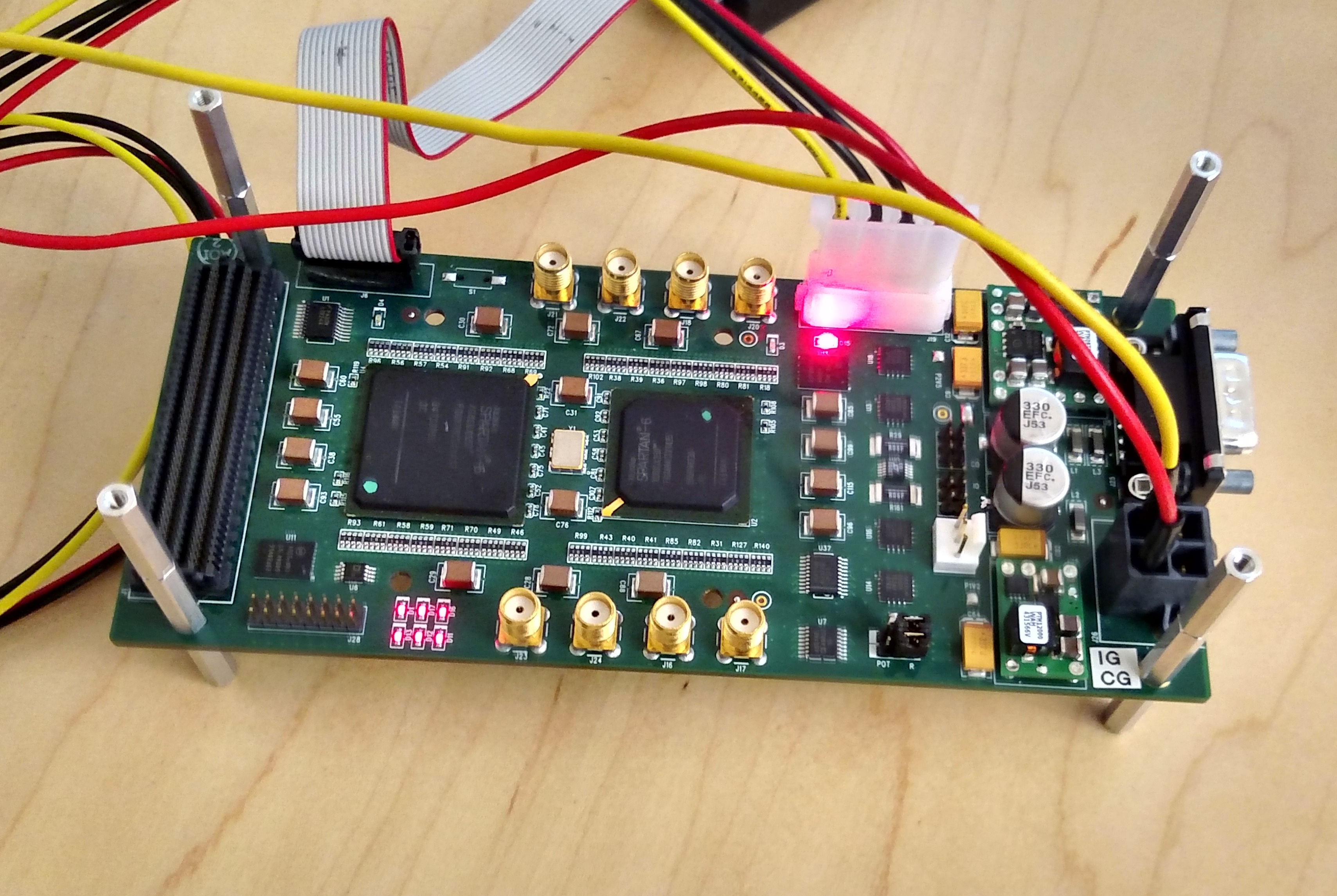
The board has been tested and is up and running in our lab.
Version 1 of the board is a 14-layer impedance-controlled board, designed with Mentorgraphics PADS.
It offers some tweaks for better power integrity (capacitors, 14-layers with better stackup and plane arrangement)
as well as optimized capacitor sizing and placement.
Send us email for a pointer to the repo with the files.
(We want to make sure you get all the help you need as an early adopter.)
BaseJump SuperTrouble
This motherboard implements Socket 352 that is mapped onto the DARPA CRAFT 600+ pin FC-BGA (flip chip BGA) package.
SuperTrouble V2 is now up and running in our lab, and features a 30A power supply circuit.
The design will be uploaded to the repo soon.
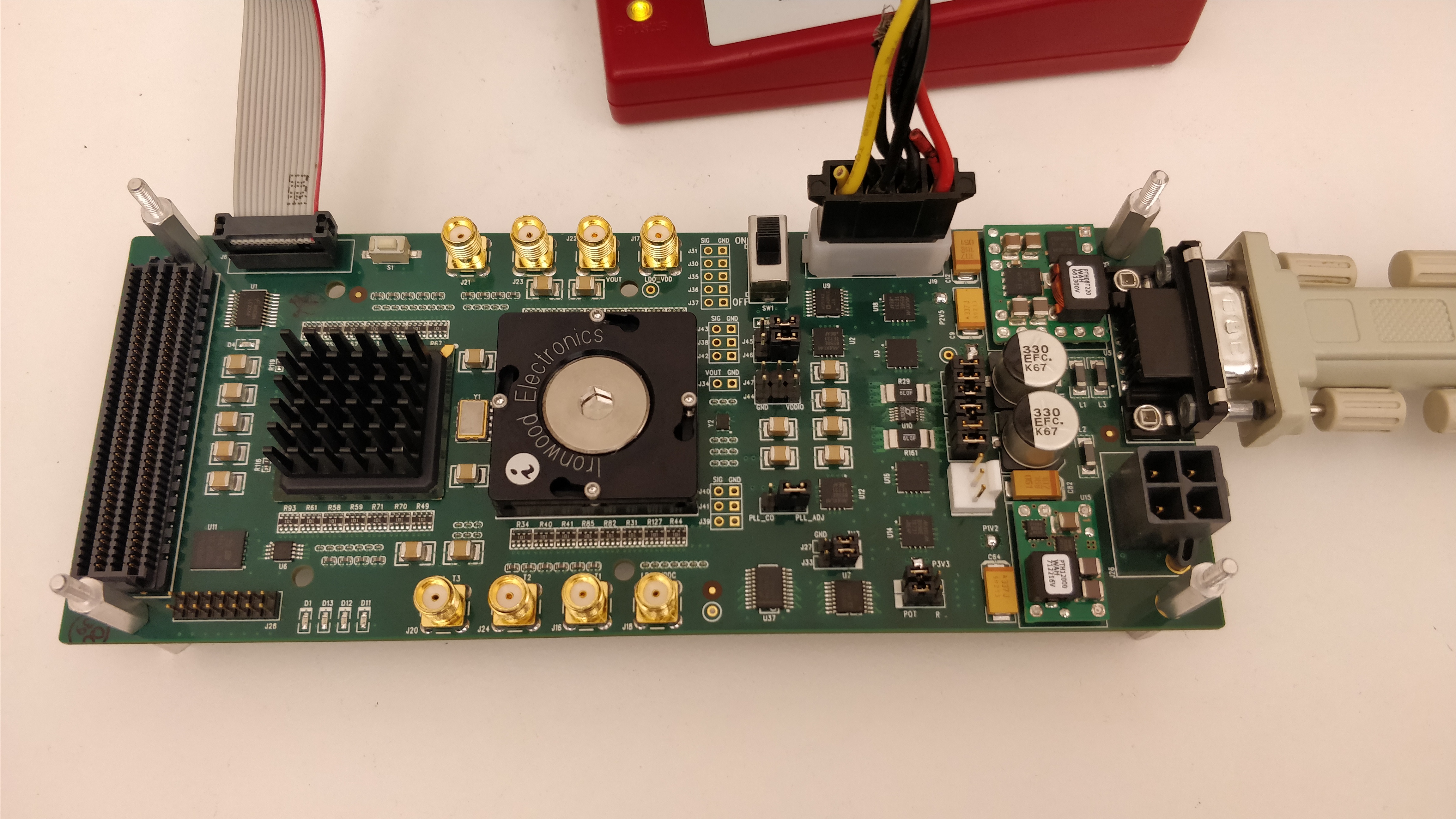
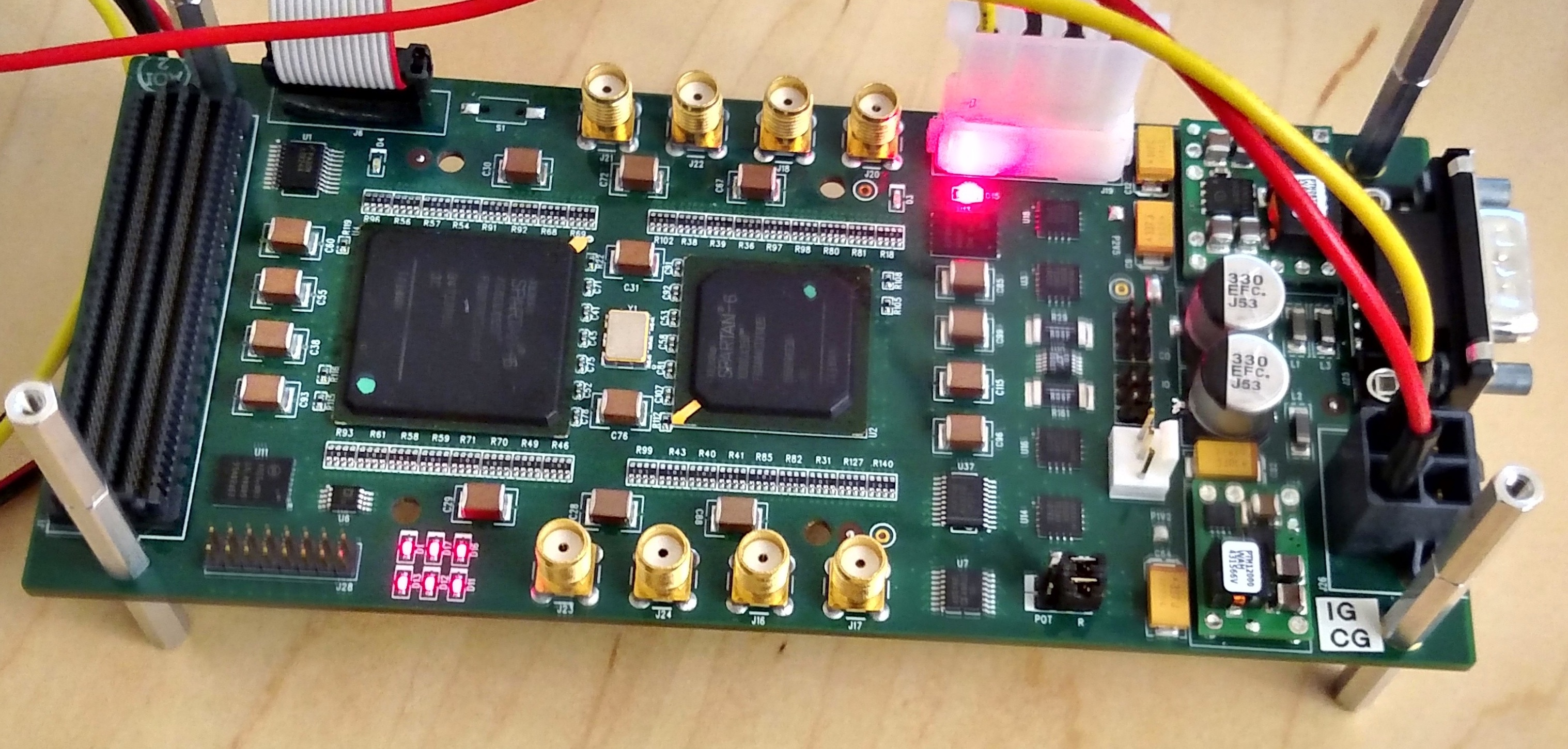
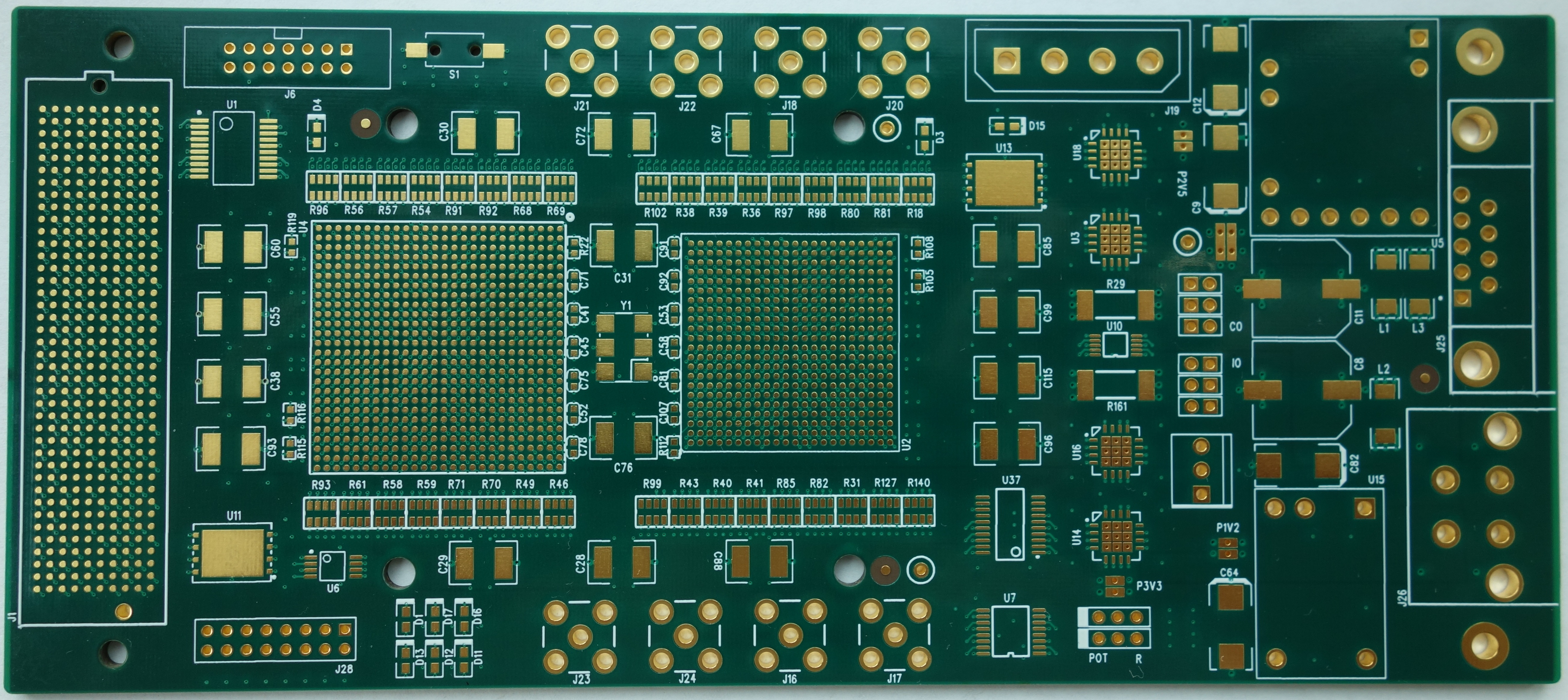
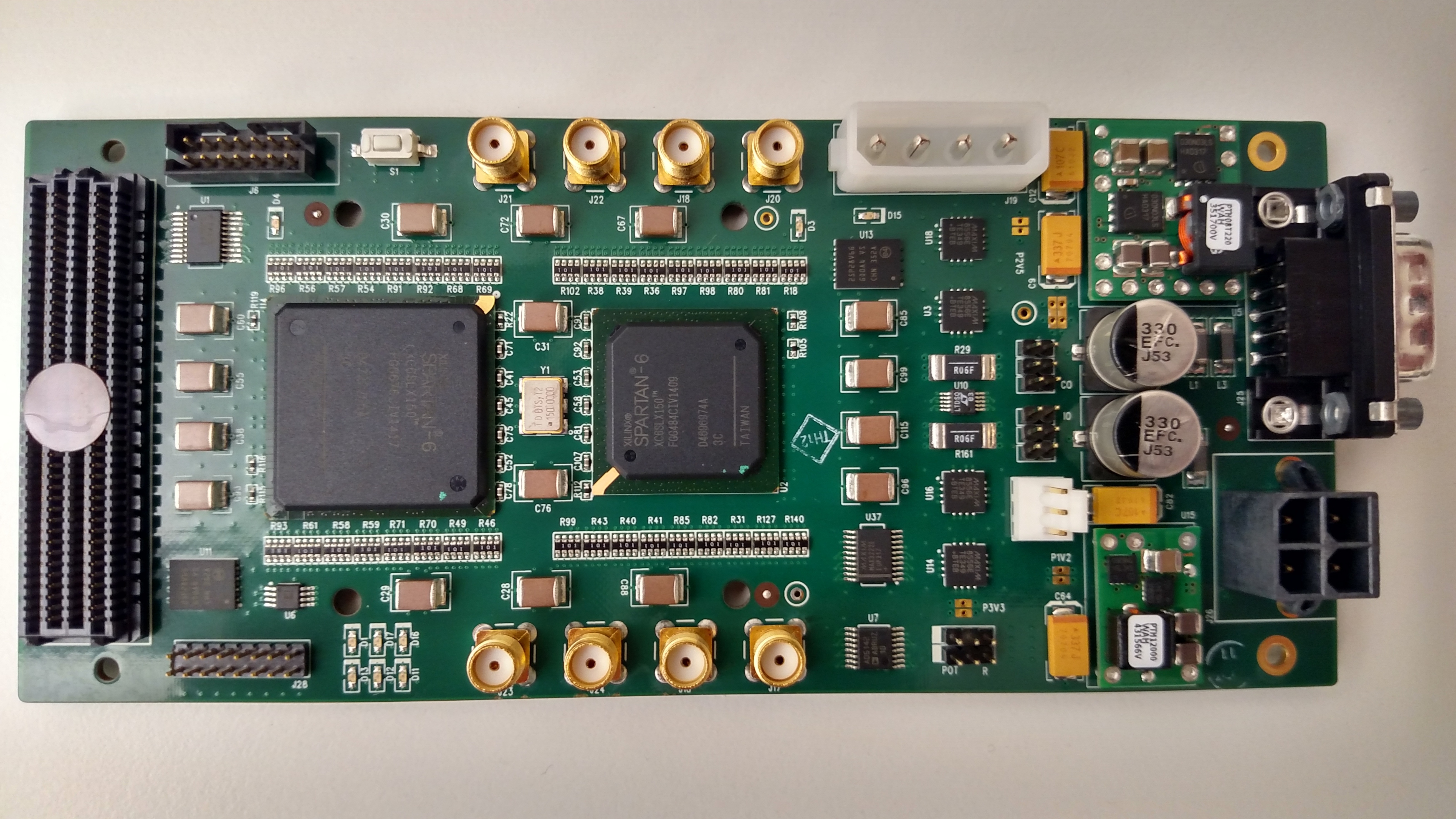
BSG DoubleTrouble (Motherboard with Socket 352 ASIC emulation)
This daughterboard design is largely identical to the Double Trouble board
but instead uses a BaseJump Socket 352 BGA instead of an emulation FPGA.
The board has been tested and is up and running in our lab.
Before taping out your chip, you can emulate both your FPGA-firmware
and your ASIC verilog code, using the Double Trouble daughterboard.
The Double Trouble Daughterboard has two Spartan-6 FPGAs, referred to as
the "Gateway FPGA" and the "ASIC FPGA". The ASIC FPGA is replaced
by your real ASIC chip in the "Real Trouble" Daughterboard.
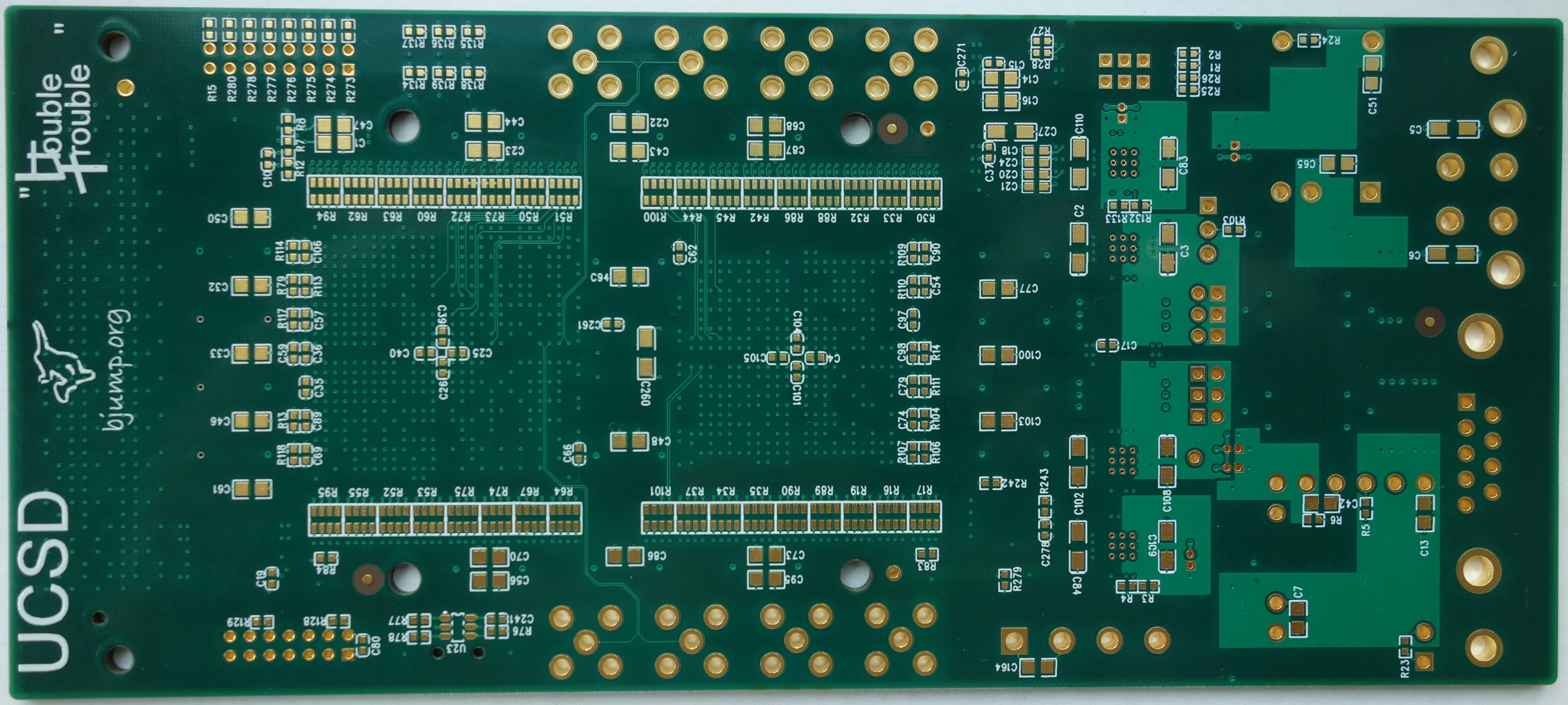
Version 1.2 of the board is a 14-layer impedance-controlled board, designed with Mentorgraphics PADS.
It offers some tweaks for better power integrity (capacitors, 14-layers with better stackup and plane arrangement)
as well as optimized capacitor sizing and placement.

Version 1.0 of the board is 10-layer impedance-controlled board, designed with Mentorgraphics PADS.


View the BaseJump Double Trouble Design Document.
View the BaseJump Double Trouble Version 1.00 Schematic.
View the BaseJump Double Trouble FPGA Ballouts.
View the BaseJump Double Trouble High Speed Firmware Design Document.
View the BaseJump Double Trouble V 1.0 Bootstrapping Document.
Download/view Double Trouble 1.0 Design Files.
View the Rev 1
BaseJump Double Trouble PCB Fab Quote,
BaseJump Double Trouble PCB Fab Request,
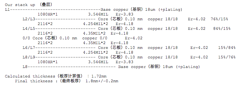
BaseJump Double Trouble Stackup (from ChinaFastPCB)
and BaseJump Double Trouble Assembly Quote (Hughes Circuits).
(Note that the PCB fab quote includes "paste cost", which is the cost of
making metal stencils for doing your own in-house assembly. We experimented with
this--we purchased some reflow ovens--but decided to go outside for it, and
they did not use the stencils.)

